
Lightning Arctic – In situ TEM Solution with Cooling/Heating and Biasing
In situ
In Situ TEM Cooling, Biasing & Heating for your TEM

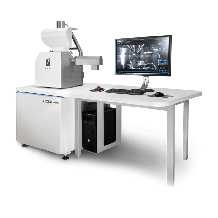
World’s most versatile and powerful tungsten SEM for both high- and low-vacuum operations
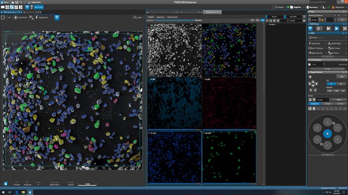
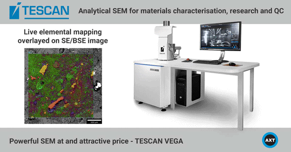
TESCAN VEGA integrates SEM imaging and optional Essence™ EDS in one live view window to make analytical operation fast and easy. Essence™ EDS is as simple as a single mouse click optimising all set-up parameters through the software, initiating elemental analysis of the sample. Fully integrated Essence provides immediate access to the elemental spectrum at any point or region, presenting the data as an elemental map or point/line EDS spectra.
An innovative optics design guarantees immediate and seamless selection of either imaging or analytical conditions as required, without the need for mechanical re-alignment of any in-colum element. Using a unique additional Intermediate Lens™ powered by TESCAN’s In-Flight Beam Tracing™, you can continuously increase beam current to a value that optimises signal to noise ratio for imaging at the desired magnifications and accelerating voltages.
Furthermore, switching from low voltage imaging mode to high voltage analytical modes is achieved with a single mouse click.
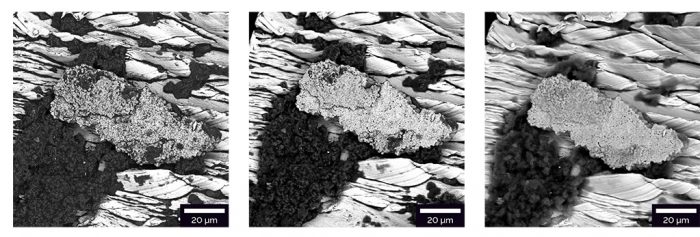
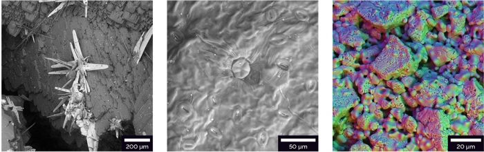
Caption – Metal fracture with a surface contamination captured at 5, 10 and 30 keV respectively. BSE information differs significantly from the increased surface sensitivity characteristic of lower accelerating energies
TESCAN’s unique Wide Field Optics™ mode provides you with a live SEM overview and a more intuitive navigation process with an unprecedented depth of field and a view o the sample’s actual topography. Continuously zoom in on your area of interest from 2x magnification using the live SEM view window.
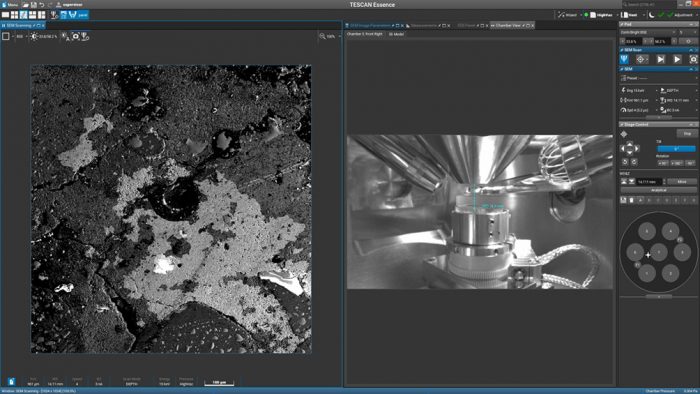
The 4th generation VEGA benefits from TESCAN’s Essence multi-user software interface which has been designed so that each user can streamline the user interface to their own specific requirements. This allows you to define workflows that match their level of experience and/or specific application need.
Caption – Essence™ software layout
Supplied as standard, SingleVac mode uses factory-preset pressure to optimise imaging conditions of charging samples without the need for conductive coatings.
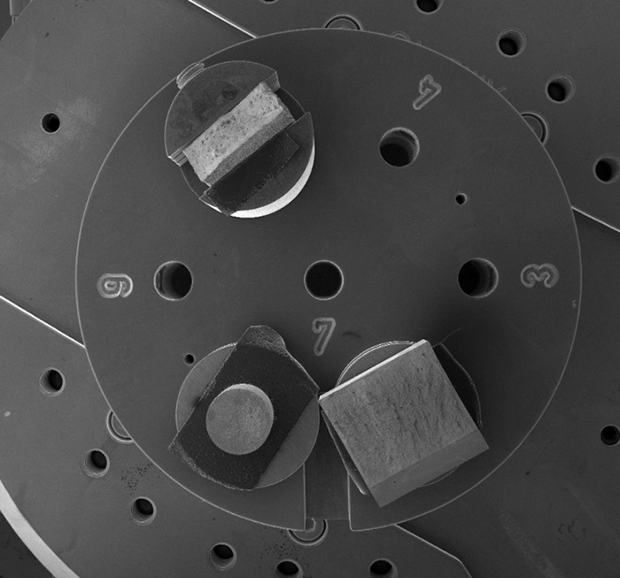
Caption – Geological sample (left); Tree leaf (middle) and Ceramic (right) imaged with 4QBSE detector Color mode
in SingleVac™ mode.
The TESCAN VEGA is a powerful SEM that can be had at an affordable price. With live EDS it has many applications including:


