Scientists, engineers, technicians and students have long wanted a TEM solution that is readily usable without weeks, or months, of training on non-productive electron-optical adjustments and alignments. TESCAN have listened and delivered the TENSOR, a 4D STEM that is as easy to use as TESCAN’s SEMs making TEM capabilities accessible by a wider audience. They have achieved this by implementing “measurements” with preset optical properties such as beam current, convergence angle, spot size and precession ON or OFF, adjusted and aligned automatically.
The TESCAN TENSOR enables multimodal characterisation of nanoscale morphological, chemical, and structural properties of functional materials, thin films and synthetic particles, with stand-out 4D-STEM performance and unprecedented usability.
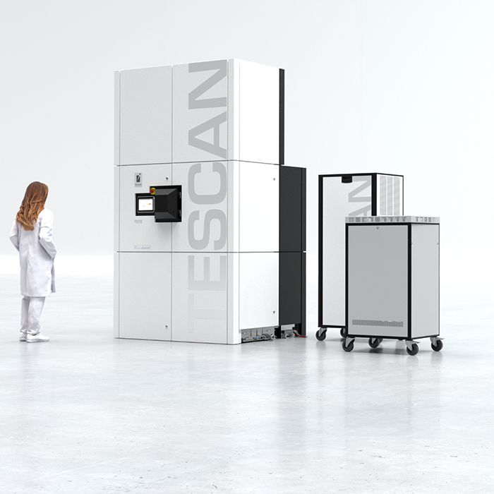
Designed from the ground up with no compromises, TESCAN TENSOR seamlessly integrates state-of-the-art components, optimised for performance.
Explore – Access to STEM and Associated Datasets
TENSOR is powered by Explore, an integrated platform for real-time processing and analysis of large-scale scanning electron diffraction datasets. With ease-of-use in mind, Explore brings 4D-STEM enables complex measurements to be made without requiring expert knowledge of STEM optics or 4D-STEM data analysis and post-processing. This helps to make the system universally attractive to anyone involved in materials science, semiconductors, failure analysis or crystallography.
Imaging and Analysis Techniques
- STEM BF (bright field), ADF (annular dark field) and HAADF (High-angle annular dark-field) Imaging
- STEM Lattice Imaging
- Composition (EDS Analysis and Elemental Mapping)
- Orientation / Phase Mapping
- Strain Mapping
- Virtual STEM
- STEM and EDS Tomography
- Diffraction Tomography