
SEMs and TEMs are commonplace in materials research providing high resolution insights into micro and nanostructures. While additional detectors can provide chemical analysis etc., electron microscopes have traditionally been restricted to static studies…….until recently.
The ability to observe samples under dynamic environments at the micron-scale at high resolution has driven the development of a range of stages and platforms that can operate within the confines and vacuum environment of SEM and TEM chambers.
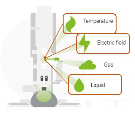
In Situ TEM Experiments
DENSsolutions manufacture a range of TEM holders that enable users to study the effects of temperature (up to 1300°C), voltage/current as well different gas and liquid environments and combinations thereof. With precision controllers, the effects on structure of these parameters can be directly seen in real time, with long-term in situ studies also possible. Furthermore, the DENSsolutions for platforms for heating and biasing are now available for SEMs with the first such system delivered to an Australian client.


In Situ SEM Experiments
For SEMs, Kammarath & Weiss offer a wide range of stages that can be located in the EM chamber to measure mechanical properties such as tensile, compression, torsion, bending and hardness. They also offer heating and cooling stages with operating ranges from liquid helium through to 1500°C as well as being able to build custom stages to suit client specific experiments. In addition to this, manipulators and probes from Kleindiek can manoeuvre and test electrical properties of materials and components at the micro-scale.


Furthermore, a range of tools and probes from Kleindeik Nanotechnik allow you to manipulate and perform in situ electrical testing within the confines of your SEM chamber. This enables you to collect data from precise locations with ease and to simultaneously image the samples in question using your SEM.


In Situ SEM and AFM
Correlative Probe and Electron Microscopy or CPEM allows simultaneous acquisition of AFM and SEM data with seamless correlation into 3D images. Through a range of different modes, AFM enables the measurement of mechanical, electrical and magnetic properties at the nanoscale as well as topography to structural information from your SEM. The LiteScope from NenoVision is compatible with most existing SEMs and further extends its capabilities.

Summary
These systems can all convert your electron microscope into a nanolaboratory capable of performing precision experiments with high-resolution imaging capabilities.