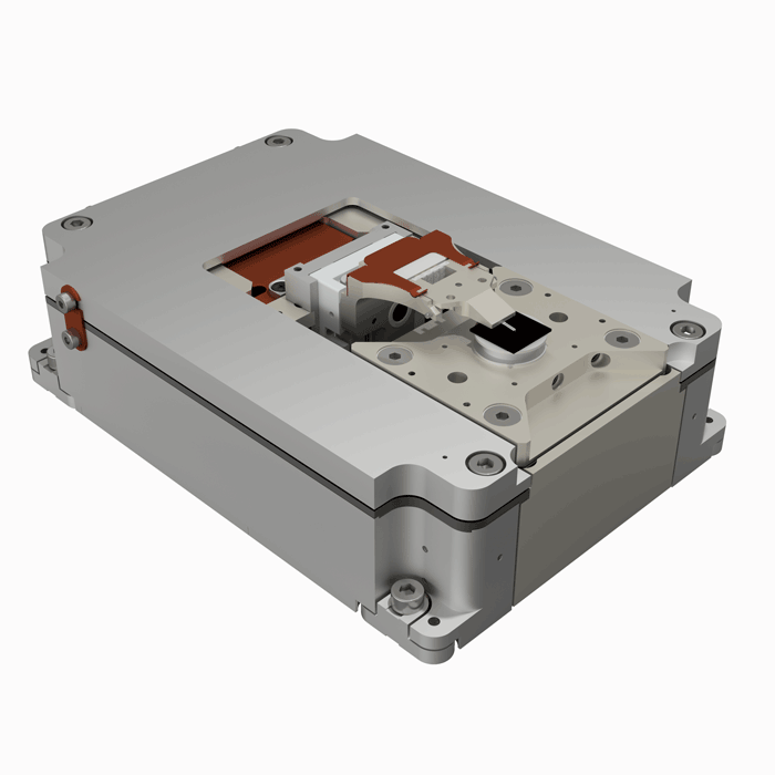
METEOR SEM METEOR is the world’s first and only fully integrated solution to optimise the cryo-ET workflow by reducing complicated transfer steps and increasing sample yield
NanoFrazor Explore Electron Beam Lithography (EBL)FabricationThermal Probe Lithography The NanoFrazor Explore has the ability to perform 3D patterning, in situ inspection, markerless overlay and high resolution Closed-Loop Lithography on nano-sized features combined with an integrated direct laser writer option for large feature patterning
XUUS4 ARPESLaser spectroscopyX-ray absorption spectroscopy (XANES/EXAFS) A bench top source for EUV and soft X-rays
RAEA Amplifier ARPESLaser spectroscopy RAEA is KMLabs' sub-25 fs, single-box amplifier. It is a fully engineered and integrated commercial source based on a single rugged optomechanical platform with a unique software-tunable repetition rate in order to maximise experiment flexibility
Cryo Module 80 Kelvin FIBIn situSEM An extremely low vibration level cryo module that runs on liquid nitrogen, adding new capabilities to your SEM
Transfer Module FIBIn situSEM Made for the purpose of carrying delicate and sensitive specimens in a capsule from the SEM into a glove box, or vice versa, to ensure they are protected from air or moisture at all times.
RH-2000 Biological MicroscopyDigital MicroscopyLight MicroscopyMicroscopy Highly Customisable digital microscope for 2D and 3D examination and analysis of samples from 0x to 10,000x magnification
TESCAN VEGA CLElectron Beam Lithography (EBL)In situMicro XRFSEMWDS Versatile and powerful tungsten SEM
Ti:Sapphire Laser Oscillators Laser spectroscopySpectrophotometry Ti:sapphire is the workhorse of ultrafast lasers due to its high gain bandwidth, enabling delivery of the shortest pulses and scalable to high pulse energy and average power. KMLabs provides a full suite of modelocked oscillators and integrated oscillator-amplifier systems, spanning pulse energies from the nJ range to 30 mJ in pulses from 15 to 40 fs.
NanoFrazor Scholar Electron Beam Lithography (EBL)FabricationThermal Probe Lithography The NanoFrazor Scholar has the ability to perform 3D patterning, in situ inspection, markerless overlay and high resolution Closed-Loop Lithography on nano-sized features in a bench top design
MM3E Micromanipulator FIBIn situSEM Adding capabilities from in situ lift-out, electrical probing (FA)and nano-manipulation, the encoded MM3E micro-manipulator brings new functionality to your SEM or FIB/SEM instrument
Lightning In situTEM In Situ TEM Biasing & Heating Sample Dynamics under controlled electrical and thermal environment.
NanoWorkstation FIBIn situSEM The NanoWorkstation is a powerful, dedicated system that allows physical manipulation and characterisation at the micro and nano-scale with ease adding new capabilities to your SEM or FIB/SEM instrument.
ProbeWorkstation FIBIn situSEM The ProbeWorkstation is a powerful, dedicated system for electrical characterisation of semiconductor devices and advanced materials in SEM and FIB. The optimal combination of our market-leading nano-manipulation and probing products provide a versatile, integrated solution for failure analysis and R&D applications requiring stable, low-current measurements.