
MEMS-based TEM platforms that enable dynamic studies under variable heating, biasing, gas and liquid conditions and combinations thereof are not uncommon. However, similar systems for use in SEMs have not been documented and have not been commercially available ……. until now.
Platforms for TEMs allow true dynamic, in situ studies to be performed whereby researchers can observe and take measurements during an entire process. This has the distinct advantage over more static studies, where a sample may be subjected to a stimuli and examined post mortem, requiring possible changes to be inferred and valuable information to potentially be missed e.g. where transformations are reversible. Furthermore, where changes are irreversible or where there may be multiple transformations, dynamic in situ studies can potentially accelerate your research and development program and save on samples and sample preparation, which can be significant when working with exotic materials. In this arena, DENSsolutions have been a world leader designing and manufacturing in situ TEM platforms.
With a strong interest in TKD (Transmission Kikuchi Diffraction) borne from seminal research published by Pat Trimby in 2012 (10.1016/j.ultramic.2012.06.004) and in-house expertise lead by SEM Manager Dr. Vijay Bhatia, the team at the University of Sydney was a logical choice to collaborate with to develop a TKD stage for SEMs, and thus a collaboration was established. What ensued was a valuable exchange of ideas, engineering drawings and prototypes adapting in situ TEM technology for SEM, and combining it with the versatility of TKD. After a relatively short development program aided by considerable knowledge of the technique and technology, the team produced the in situ TKD stage that allows researchers to perform dynamic studies under variable biasing and temperature conditions. This collaboration led to a join publication which will be available soon online. This product is now commercially available through DENSsolutions.
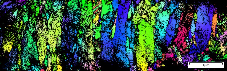
When asked about the impetus behind developing this new product, Dr. Bhatia replied, “interest in TKD has been increasing in recent times with its ability to generate orientation maps of electron transparent materials and to map changes in crystal orientation or structure in nanocrystalline materials across micron-sized regions with 4 nm resolution ensuring statistically relevant analyses. This has seen TKD applied to an expanding range of applications. The possibility of performing TKD studies in an SEM offers a lower cost alternative to TEM as well as a simpler workflow pathway. Add to this the potential to use it as a screening tool for high-resolution TEM and even atom probe studies and TKD in SEM becomes an even more versatile and valuable tool for materials researchers.”
Speaking about the product development experience, Dr. Bhatia added, “working with the team at DENSsolutions was a very rewarding experience. We are proud to know that our team has directly contributed to the development of a commercially available product and that it will help TKD become a more widely used analytical technique as a result. In situ experiments are a key focus at SMM and this technology allowed us to combine the two areas of expertise”.
In response, Dr. Hugo Pérez-Garza, Chief Technology Officer at DENSsolutions commented, “we value working with researchers and collaborators with expertise in fields that are complimentary to our own. This collaboration with the team at the University of Sydney is yet another example of a successful collaboration and we are extremely grateful to them for their valuable contributions.”
The in situ TKD platform for SEMs jointly developed by the University of Sydney and DENSsolutions is now available for purchase. It is available in two variants suitable for JEOL and FEI-Thermo SEMs and FIB-SEMs and is compatible with both, EBSD and TKD detectors:
- Wildfire – offering heating from room temperature to 1200°C
- Lightning – Biasing 0 to 150V with the option of heating to 900°C
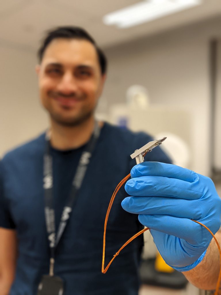
The in situ TKD stage also features a modular design in that the MEMS chip or Nano-Chip™ is interchangeable with DENSsolutions’ TEM platforms enabling you to carry out dynamic in situ heating and/or biasing experiments in your TEM with the corresponding TEM holder.
There were advantages to using the same Nano-Chip for SEM and TEM platforms. From a product development perspective, using an existing component reduced the developmental timeframe, plus the performance of the MEMS chip was well known. From a users’ perspective, you now have the flexibility of being able to take your sample (with the Nano-Chip) seamlessly from SEM to TEM or vice versa. This gives you to the ability to correlate structural and morphological changes from dynamic SEM studies with atomic-scale changes during dynamic TEM studies, allowing you to more thoroughly understand how your materials and specimens behave.
DENSsolutions have already demonstrated great experience with the use of Nano-Chips where they have already developed several products that have enjoyed commercial success:


Authors
Dr. Cameron Chai1, Dr. Vijay Bhatia2, Dr. Kamran Khajehpour1, Dr. Hugo Pérez-Garza3 and Dr. Yevheniy Pivak3
1. AXT PTY LTD, Australia
2. Sydney Microscopy and Microanalysis, University of Sydney, Australia
3. DENSsolutions, The Netherlands