
SEM has been a pillar for scientific research for many years revealing structural details about materials, organisms and systems that would otherwise remain invisible. Modern systems produce ultra-high-resolution 2D images at magnifications that can exceed 2,000,000 times. Continued development of SEMs have seen the technology become more widely applied through lower barriers to implementation, as well as increased reliability and usability as well as integration with other techniques such as FIBs.
Correlative and Complementary Analytical and Imaging Techniques
There is a growing trend towards using complimentary techniques to generate more comprehensive analyses of a material or system. While some combinations like SEM with EDS have been used (for what seems like) forever, other combinations are emerging that generate complimentary datasets that can be correlated, resulting in a more definitive understanding of the sample in question. Many of these can be performed in situ and even simultaneously, effectively fast-tracking your research.
As mentioned, SEMs provide highly detailed 2D images of sample surfaces. But what if you wanted to learn more about its topography? Or what if you wanted to learn about the mechanical or electrical properties of your material at the nanosclale? What if you could do all this inside your SEM?
In Situ AFM for your SEM – CPEM
The good news is this is now possible. The LiteScope from Nenovision is an AFM designed to fit inside your SEM and using Correlative Probe and Electron Microscopy or CPEM, you can correlate nanometre-resolution topographical information with your SEM images in a time-efficient manner and generate 3D images. Furthermore, being able to perform both SEM and AFM measurements together not only saves you time, but it also removes any possible experimental variables associated with moving your sample or measuring under different conditions.
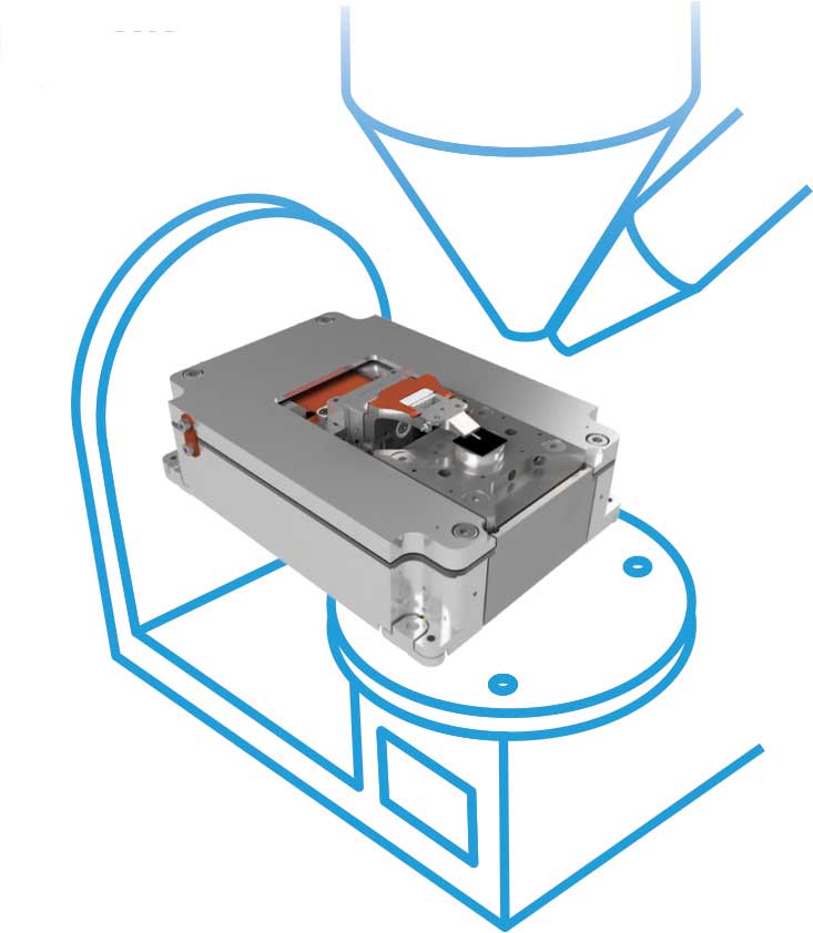
Schemnatic of LiteScope AFM in an SEM chamber.
Applications of CPEM
CPEM has applications across a range of scientific fields including:
| Nanoscience | Materials Science | Life Science | Semiconductors |
|---|---|---|---|
| Modified surfaces FIB/GIS Quantum dots Nanostructured films Nano-patterning Nanowires | 1D / 2D materials Steel & metal alloys Batteries Ceramics Polymers & Composites | Cell biology Marine biology Protein technology | Integrated circuits Solar cells MEMS / NEMS Failure analyses Dopant visualization Current leakage localisation |
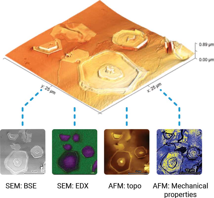
Complex analysis of 2D Materials
In the analysis of molybdenum carbide Mo2C. the SEM with LiteScope quickly delivers topography, EDX, and mechanical properties.
- CPEM – precise correlation of chosen AFM and SEM data
- SEM-EDX: fast nanostructure localization and elemental analysis
- AFM: topography, conductivity, mechanical properties
Correlative analysis of the same spot of the Mo2C squares using increasing ion dose. The interface of the FIB induced
paramagnetic to ferromagnetic transformation is highlighted.
In Situ Analysis of Sensitive Materials
The in situ nature of the LiteScope platform lends itself to magnetic nanopatterning. With the LiteScope it is possible to selectively change magnetic properties using your FIB to induce transformation and to characterise magnetic properties, even in metastable Fe78N22 thin films.
- FIB – induced transformation of a sensitive sample
- AFM – identified precisely the ROI and analysed the feature
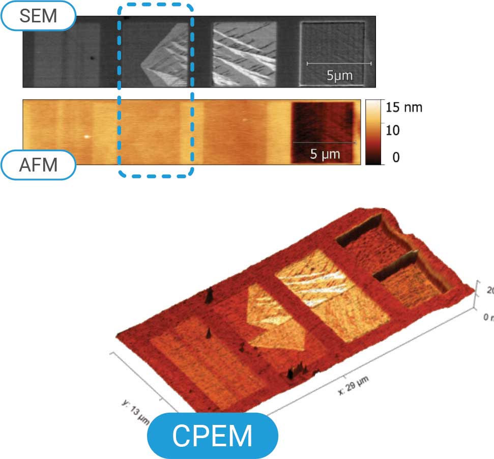
SEM image, AFM image, and 3D CPEM view of FIB milled squares using increasing ion dose. The interface of the FIB induced
paramagnetic to ferromagnetic transformation is highlighted.
In Situ Analysis of Sensitive Materials
The in situ nature of the LiteScope platform lends itself to magnetic nanopatterning. With the LiteScope it is possible to selectively change magnetic properties using your FIB to induce transformation and to characterise magnetic properties, even in metastable Fe78N22 thin films.
- FIB – induced transformation of a sensitive sample
- AFM – identified precisely the ROI and analysed the feature
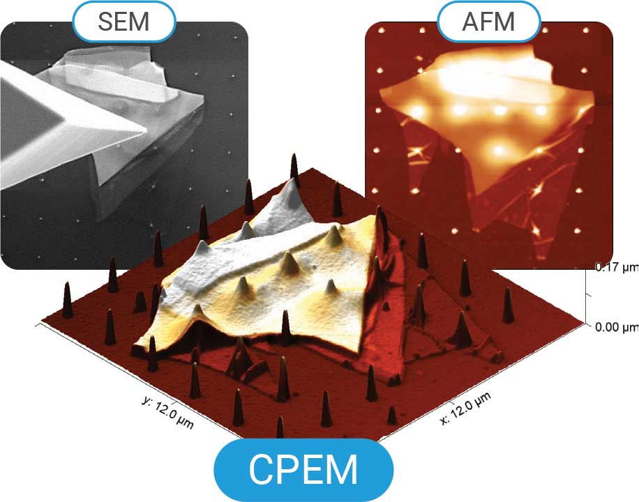
SEM image, AFM image, and 3D CPEM view of WSe2.