
A development in semiconductor device delayering by broad argon ion beam milling [Model 1062 TrionMill, Fischione Instruments] offers an effective milling area of up to 50 mm. The ability to fully control the delayering process is critical, especially for fully fabricated wafers, where the final aluminum pads, lines, and passivation have significant thickness.
A milling area of this size is made possible by the user’s ability to position each of the tool’s three ion beams individually. This flexibility in ion beam positioning also enables more precise targeting of an area of interest. The beam emission parameters can be individually adjusted for each ion source, which allows the user to control the beam size and beam current. The delayering strategy can be adapted to meet the investigator’s goals.
We targeted and delayered a 2 mm diameter area, using a fully fabricated wafer that contained both logic and memory. The three ion beams were configured specifically for delayering, which is an off-center alignment. The beam energy was 6 keV (left and right beam) and 5.5 keV (center beam); the beam current and beam width were specifically tuned for each ion source. These parameters allow uniform milling over a millimeter-scale area by compensating for the ion beams continuously striking the center of the sample during stage rotation.
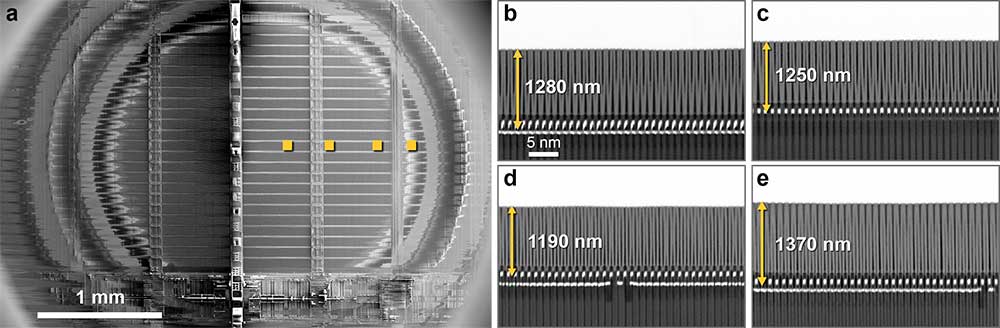
Figure 1a is a SEM image of the delayered area. The delayered area is 2 mm diameter and is extremely clean and uniform. The slope area, which exposed the silicon nitrate, silicon oxide, aluminum, and copper layers, is more than 4 mm (as measured from the center of the delayered area). To quantify the uniformity of the delayered area, FIB cross-section samples were taken from different points across the milling area (Fig. 1b‑e). The FIB cross-section samples and measurements of the remaining layers thicknesses show ± 130 nm uniformity of delayering across a 2 mm diameter area.
The results highlight that broad argon ion beam milling, after removing approximately 5 µm of device material (including the top thick passivation and aluminum layers), produces excellent surface quality over a millimeter-scale area.