On-demand webinar
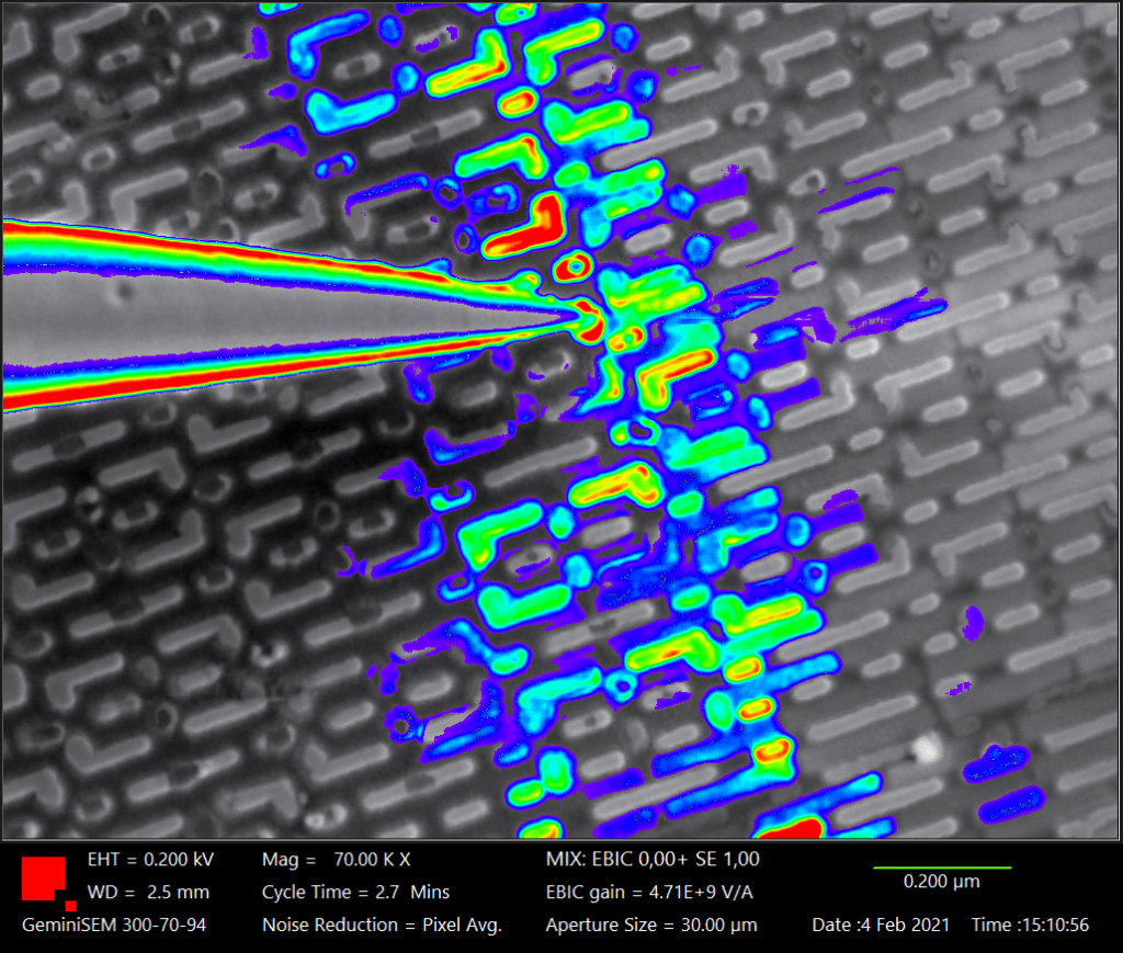
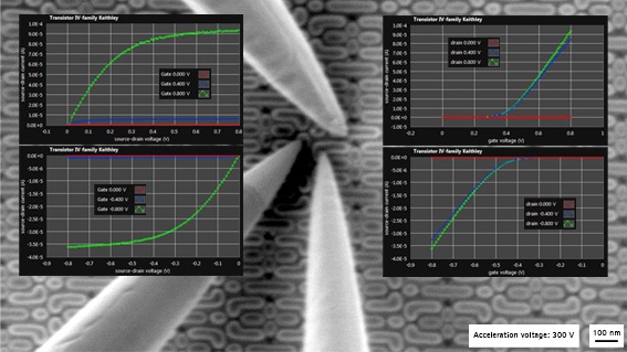
When it comes to nanoscale characterisation of electrical and mechanical properties of materials or devices, Kleindiek have amassed almost 25 years of expertise. In this time, they have developed a portfolio of unique nanomanipulators, substages, and additional in situ tools. These tools continue to open up a broad range of applications that can be achieved inside SEM or FIB/SEM chambers. Combining sub-atomic precision and very high stability, researchers are able to perform delicate operations interacting with the nano world with ease.
As technology pushes further into the nano realms and materials and performance demands intensify, these systems have enabled researchers to keep pace. In this webinar several examples will be demonstrated and discussed including solar cells, battery materials, microelectronics, MEMS and more, which will no doubt provide inspiration of how this technology can be applied to your own research projects.
Watch the webinar
Presenter – Dr. Andrew Smith
Sales & Application Specialist, Kleindiek Nanotechnik
Andrew studied chemistry at the Heinrich-Heine-Universität Düsseldorf, and after focussing on electrochemistry for his Master thesis, he completed his PhD at the Max-Planck-Institute for Iron Research where he investigated single crystalline metallic nanowires. This is where he came into contact with Kleindiek Nanotechnik’s systems. Right after defending his thesis, he joined Kleindiek Nanotechnik in an app development and sales capacity.