
TESCAN ORSAY HOLDING a.s. announces the release of their Essence™ EBL Kit, a fully integrated, dedicated solution that adds electron beam lithography capabilities to TESCAN SEM and FIB-SEM instruments. Working in conjunction with TESCAN’s fast electrostatic beam blanker, the Essence™ EBL Kit offers a pathway for multi-user research labs to fulfill requirements for prototyping microand nanoscale structures and devices while also providing access to the imaging and analysis capabilities of SEM and FIB-SEM.
 TESCAN ORSAY HOLDING a.s. announces the release of their Essence™ EBL Kit, a fully integrated, dedicated solution that adds electron beam lithography capabilities to TESCAN SEM and FIB-SEM instruments. Working in conjunction with TESCAN’s fast electrostatic beam blanker, the Essence™ EBL Kit offers a pathway for multi-user research labs to fulfill requirements for prototyping microand nanoscale structures and devices while also providing access to the imaging and analysis capabilities of SEM and FIB-SEM.
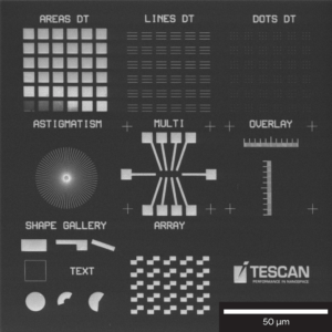
Electron beam lithography is a technique that uses a focused beam of electrons to draw patterns on a surface covered with an electron-sensitive film (resist). This technique is common in prototyping for preparation of micro- and nanostructures with specific shapes, dimensions and material composition on various substrates, such as sensors, photonics, plasmonics, spintronics, MEMS, microfluidics, and surfaces for cell growth.
“Within small scientific research groups at a university or other institution, instruments often are shared by multiple groups so versatility, ease of use and reliability are major concerns when acquiring new equipment,” states Tomáš Šamořil, Product Manager Special Applications – NanoPrototyping, ToF-SIMS. “By expanding the capabilities of SEM or FIB-SEM to include intermediate-level electron beam lithography applications, TESCAN SEM and FIB-SEM instruments are able to fulfill the needs for both characterization and prototyping.” Adding electron beam lithography to a SEM or FIB-SEM allows researchers to capitalize on the analytical capabilities of either platform after completing the lithography process to validate structures, dimensions or material composition. EBL together with precision material removal provided by focused ion beam (FIB) and gas injection system (GIS) technology is proven to be a powerful combination for fast prototyping of micro- and nanodevices within photonics, optics, plasmonics, magnetism, biology, and electronics.
TESCAN Essence™ EBL Kit includes a software module that is fully integrated with TESCAN’s Essence™ microscope control software and uses the open source, third party pattern editor KLayout to execute all the required lithography steps. This makes operation easy as well as streamlining mixed-technology design processes without complicated data handling.