
AttoMap
Micro XRF
The Most Advanced XRF Microscope Assembled for a Homelab

We describe a new technique for non-destructive, quantitative measurements of dopants with equivalent thicknesses below 1 Angstrom and high-fidelity measurements of thin films, and with spatial resolutions of 10 μm. The need for such a system is driven by advances in materials science and semiconductor, such as 3D finFETs. Sigray’s AttoMap MicroXRF provides ultra-high sensitivity at high throughput for measurements well below sub-angstrom concentrations for elements such as Hf, Ni, Co, and has demonstrated <1% repeatability for 1-2 nm thicknesses measured within 2 minutes.
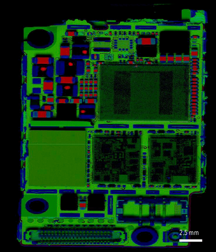
iPhone Chip
Phone chip with buried copper (green) layers visualized non-destructively, without removing the epoxy resin covering
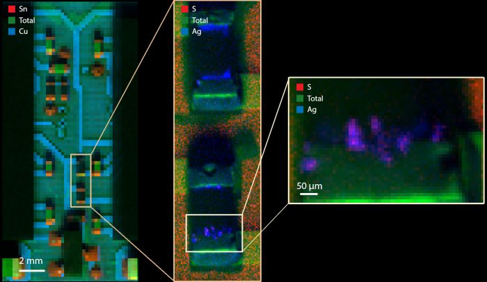
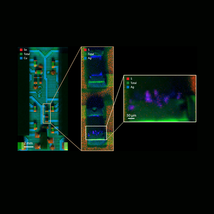
Rapid Semiconductor Contamination Detection
Extremely fast scans were performed to locate suspected sulfur contamination of silver resistor conductors.
Left: A survey scan was first performed to locate the regions of silver.
Middle: A higher resolution scan was used to locate suspected sulfur contamination.
Right: Final scan was used to verify and revealed that Silver-sulfide was forming crystals and distorting the silver structure.
The scans provide a fast and non-destructive alternative to the labor-intensive, destructive cross-sectioning methods employed previously. Moreover, it also pinpointed new unexpected regions of incipient resistor breakdown.
